The Metal Oxide FET - MOSFET
As well as the Junction Field Effect Transistor (JFET), there is another type of Field Effect Transistor available whose Gate input is electrically insulated from the main current carrying channel and is therefore called an Insulated Gate Field Effect Transistor or IGFET. The most common type of insulated gate FET which is used in many different types of electronic circuits is called the Metal Oxide Semiconductor Field Effect Transistor or MOSFET for short.
The IGFET or MOSFET is a voltage controlled field effect transistor that differs from a JFET in that it has a "Metal Oxide" Gate electrode which is electrically insulated from the main semiconductor N-channel or P-channel by a thin layer of insulating material usually silicon dioxide (commonly known as glass). This insulated metal gate electrode can be thought of as one plate of a capacitor. The isolation of the controlling Gate makes the input resistance of the MOSFET extremely high in the Mega-ohms ( MΩ ) region thereby making it almost infinite.
As the Gate terminal is isolated from the main current carrying channel "NO current flows into the gate" and just like the JFET, the MOSFET also acts like a voltage controlled resistor were the current flowing through the main channel between the Drain and Source is proportional to the input voltage. Also like the JFET, this very high input resistance can easily accumulate large amounts of static charge resulting in the MOSFET becoming easily damaged unless carefully handled or protected.
Like the previous JFET tutorial, MOSFETs are three terminal devices with a Gate, Drain and Source and both P-channel (PMOS) and N-channel (NMOS) MOSFETs are available. The main difference this time is that MOSFETs are available in two basic forms:
- 1. Depletion Type - the transistor requires the Gate-Source voltage, ( VGS ) to switch the device "OFF". The depletion mode MOSFET is equivalent to a "Normally Closed" switch.
-
- 2. Enhancement Type - the transistor requires a Gate-Source voltage, ( VGS ) to switch the device "ON". The enhancement mode MOSFET is equivalent to a "Normally Open" switch.
The symbols and basic construction for both configurations of MOSFETs are shown below.
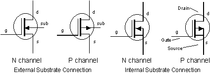
The four MOSFET symbols above show an additional terminal called the Substrate and is not normally used as either an input or an output connection but instead it is used for grounding the substrate. It connects to the main semiconductive channel through a diode junction to the body or metal tab of the MOSFET. In discrete type MOSFETs, this substrate lead is connected internally to the source terminal. When this is the case, as in enhancement types it is omitted from the symbol. The line between the drain and source connections represents the semiconductive channel. If this is a solid unbroken line then this represents a "Depletion" (normally closed) type MOSFET and if the channel line is shown dotted or broken it is an "Enhancement" (normally open) type MOSFET. The direction of the arrow indicates either a P-channel or an N-channel device.
Basic MOSFET Structure and Symbol
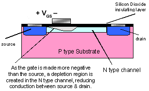
The construction of the Metal Oxide Semiconductor FET is very different to that of the Junction FET. Both the Depletion and Enhancement type MOSFETs use an electrical field produced by a gate voltage to alter the flow of charge carriers, electrons for N-channel or holes for P-channel, through the semiconductive drain-source channel. The gate electrode is placed on top of a very thin insulating layer and there are a pair of small N-type regions just under the drain and source electrodes.
We saw in the previous tutorial, that the gate of a JFET must be biased in such a way as to forward-bias the PN-junction but with a insulated gate MOSFET device no such limitations apply so it is possible to bias the gate of a MOSFET in either polarity, +ve or -ve. This makes MOSFETs especially valuable as electronic switches or to make logic gates because with no bias they are normally non-conducting and this high gate input resistance means that very little or no control current is needed as MOSFETs are voltage controlled devices. Both the P-channel and the N-channel MOSFETs are available in two basic forms, the Enhancement type and the Depletion type.
Depletion-mode MOSFET
The Depletion-mode MOSFET, which is less common than the enhancement types is normally switched "ON" without the application of a gate bias voltage making it a "normally-closed" device. However, a gate to source voltage ( VGS ) will switch the device "OFF". Similar to the JFET types. For an N-channel MOSFET, a "positive" gate voltage widens the channel, increasing the flow of the drain current and decreasing the drain current as the gate voltage goes more negative. In other words, for an N-channel depletion mode MOSFET: +VGS means more electrons and more current. While a -VGS means less electrons and less current. The opposite is also true for the P-channel types. Then the depletion mode MOSFET is equivalent to a "normally-closed" switch.
Depletion-mode N-Channel MOSFET and circuit Symbols
The depletion-mode MOSFET is constructed in a similar way to their JFET transistor counterparts were the drain-source channel is inherently conductive with the electrons and holes already present within the N-type or P-type channel. This doping of the channel produces a conducting path of low resistance between the Drain and Source with zero Gate bias.
Enhancement-mode MOSFET
The more common Enhancement-mode MOSFET is the reverse of the depletion-mode type. Here the conducting channel is lightly doped or even undoped making it non-conductive. This results in the device being normally "OFF" when the gate bias voltage is equal to zero.
A drain current will only flow when a gate voltage ( VGS ) is applied to the gate terminal greater than the threshold voltage ( VTH ) level in which conductance takes place making it a transconductance device. This positive +ve gate voltage pushes away the holes within the channel attracting electrons towards the oxide layer and thereby increasing the thickness of the channel allowing current to flow. This is why this kind of transistor is called an enhancement mode device as the gate voltage enhances the channel.
Increasing this positive gate voltage will cause the channel resistance to decrease further causing an increase in the drain current, ID through the channel. In other words, for an N-channel enhancement mode MOSFET: +VGS turns the transistor "ON", while a zero or -VGS turns the transistor "OFF". Then, the enhancement-mode MOSFET is equivalent to a "normally-open" switch.
Enhancement-mode N-Channel MOSFET and circuit Symbols
Enhancement-mode MOSFETs make excellent electronics switches due to their low "ON" resistance and extremely high "OFF" resistance as well as their infinitely high gate resistance. Enhancement-mode MOSFETs are used in integrated circuits to produce CMOS type
Logic Gates and power switching circuits in the form of as PMOS (P-channel) and NMOS (N-channel) gates. CMOS actually stands for
Complementary MOS meaning that the logic device has both PMOS and NMOS within its design.
The MOSFET Amplifier
Just like the previous Junction Field Effect transistor, MOSFETs can be used to make single stage class A amplifier circuits with the Enhancement mode N-channel MOSFET common source amplifier being the most popular circuit. The depletion mode MOSFET amplifiers are very similar to the JFET amplifiers, except that the MOSFET has a much higher input impedance. This high input impedance is controlled by the gate biasing resistive network formed by R1 and R2. Also, the output signal for the enhancement mode common source MOSFET amplifier is inverted because when VG is low the transistor is switched "OFF" and VD (Vout) is high. When VG is high the transistor is switched "ON" and VD (Vout) is low as shown.
Enhancement-mode N-Channel MOSFET Amplifier
The DC biasing of this common source (CS) MOSFET amplifier circuit is virtually identical to the JFET amplifier. The MOSFET circuit is biased in class A mode by the voltage divider network formed by resistors R1 and R2. The AC input resistance is given as RIN = RG = 1MΩ.
Metal Oxide Semiconductor Field Effect Transistors are three terminal active devices made from different semiconductor materials that can act as either an insulator or a conductor by the application of a small signal voltage. The MOSFETs ability to change between these two states enables it to have two basic functions: "switching" (digital electronics) or "amplification" (analogue electronics). Then MOSFETs have the ability to operate within three different regions:
- 1. Cut-off Region - with VGS < Vthreshold the gate-source voltage is lower than the threshold voltage so the transistor is switched "fully-OFF" and IDS = 0, the transistor acts as an open circuit
-
- 2. Linear (Ohmic) Region - with VGS > Vthreshold and VDS > VGS the transistor is in its constant resistance region and acts like a variable resistor whose value is determined by the gate voltage, VGS
-
- 3. Saturation Region - with VGS > Vthreshold the transistor is in its constant current region and is switched "fully-ON". The current IDS = maximum as the transistor acts as a closed circuit
MOSFET Summary
The Metal Oxide Semiconductor FET, MOSFET has an extremely high input gate resistance with the current flowing through the channel between the source and drain being controlled by the gate voltage. Because of this high input impedance and gain, MOSFETs can be easily damaged by static electricity if not carefully protected or handled. MOSFETs are ideal for use as electronic switches or as common-source amplifiers as their power consumption is very small. Typical applications for MOSFETs are in Microprocessors, Memories, Calculators and Logic CMOS Gates etc.
Also, notice that a dotted or broken line within the symbol indicates a normally "OFF" enhancement type showing that "NO" current can flow through the channel when zero gate-source voltage VGS is applied. A continuous unbroken line within the symbol indicates a normally "ON" Depletion type showing that current "CAN" flow through the channel with zero gate voltage. For P-channel types the symbols are exactly the same for both types except that the arrow points outwards. This can be summarised in the following switching table.
| MOSFET type | VGS = +ve | VGS = 0 | VGS = -ve |
| N-Channel Depletion | ON | ON | OFF |
| N-Channel Enhancement | ON | OFF | OFF |
| P-Channel Depletion | OFF | ON | ON |
| P-Channel Enhancement | OFF | OFF | ON |
So for N-channel enhancement type MOSFETs, a positive gate voltage turns "ON" the transistor and with zero gate voltage, the transistor will be "OFF". For a P-channel enhancement type MOSFET, a negative gate voltage will turn "ON" the transistor and with zero gate voltage, the transistor will be "OFF". The voltage point at which the MOSFET starts to pass current through the channel is determined by the threshold voltage VTH of the device and is typical around 0.5V to 0.7V for an N-channel device and -0.5V to -0.8V for a P-channel device.
In the next tutorial about Field Effect Transistors instead of using the transistor as an amplifying device, we will look at the operation of the transistor in its saturation and cut-off regions when used as a solid-state switch. Field effect transistor switches are used in many applications to switch a DC current "ON" or "OFF" such as LED’s which require only a few milliamps at low DC voltages, or motors which require higher currents at higher voltages.

 Notice the solid bar between source and drain, indicating the presence of a conducting channel.


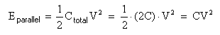
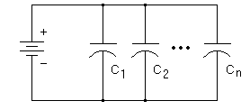 Capacitors connected in parallel will add their capacitance together.
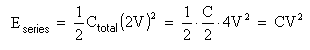
 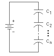 Capacitors connected in series will have a lower total capacitance than any single one in the circuit.
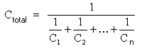 If you have only two capacitors in series this equation can be simplified to:
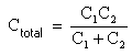 If you have two identical capacitors in series this is further simplified to:
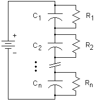 When you connect capacitors in series, any variance in values causes each one to charge at a different rate and to a different voltage. The variance can be quite large for electrolytics. On top of that, once the bank is charged, each capacitor's leakage current also causes a *different* voltage across each capacitor.